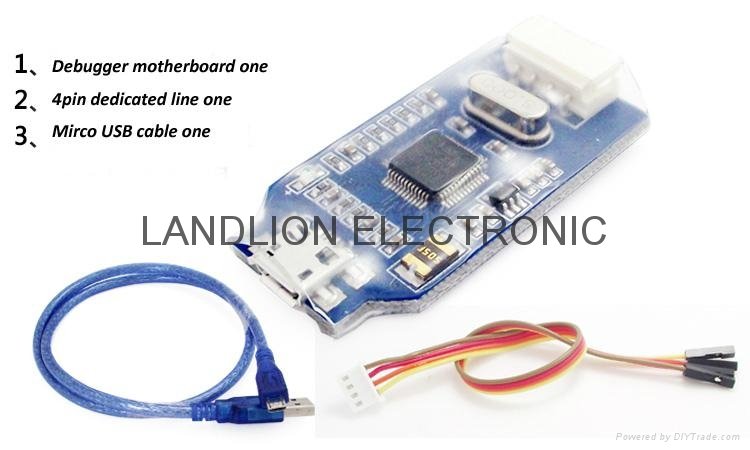
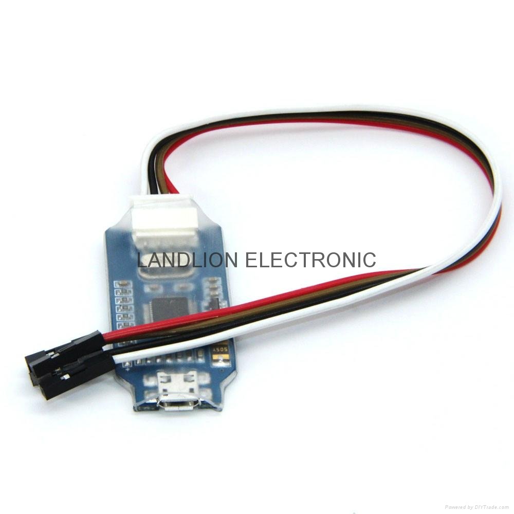
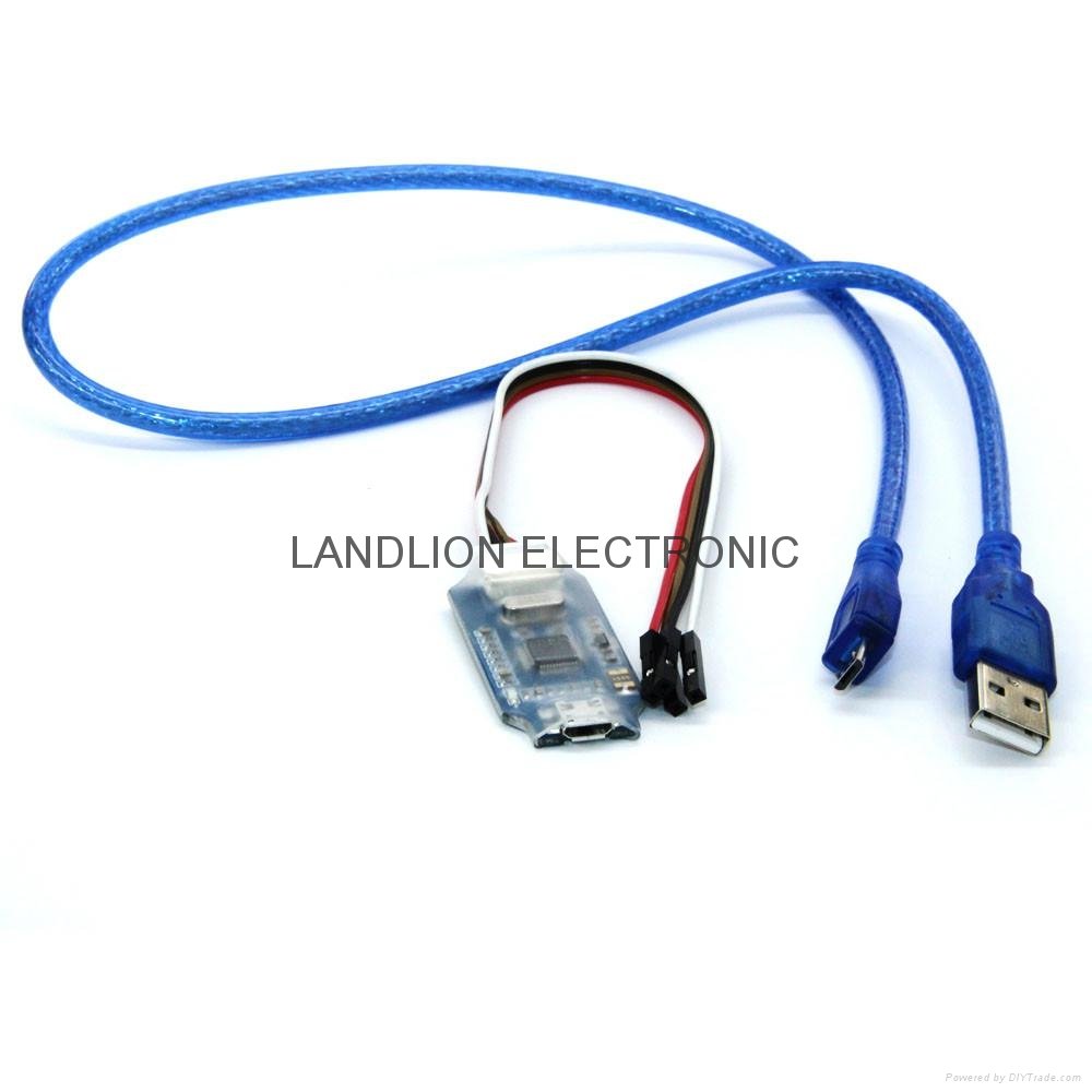
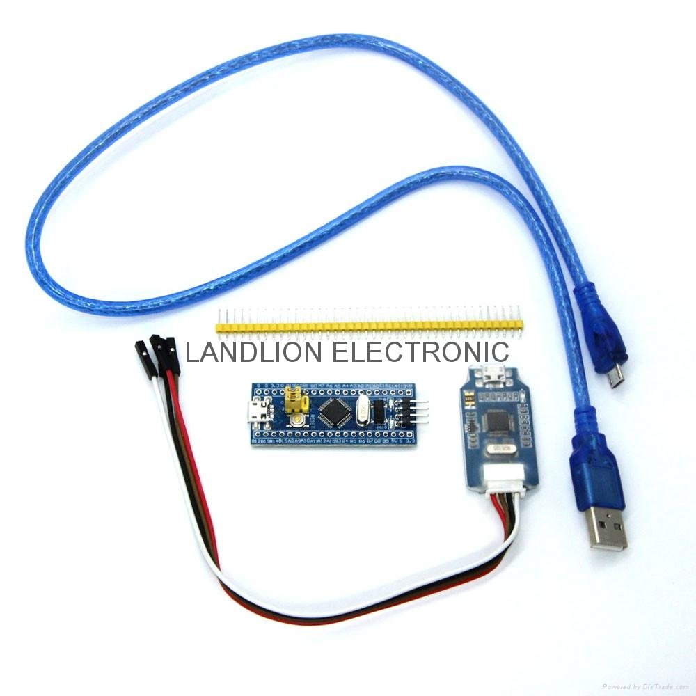
1set=STM32F103C8T6 ARM STM32 Minimum System Development Board +J-link OB ARM emu
Model No.︰STM32
Brand Name︰-
Country of Origin︰China
Unit Price︰US $ 5.98 / pc
Minimum Order︰5 pc
Product Description
J-Link-OB is a set of independent simulation debugger developed by SEGGER, which is usually designed on the evaluation board of the major companies ("on-board"), which is also the reason for the suffix "OB". The simulator called "J-Link- OB" has a USB communication function that communicates with the PC and the other end communicates with the supportable device via SWD / JTAG to complete the debug download debug task.
Our J-Link OB simulation debugger compared to the original J-Link OB less JTAG interface, leaving only the SWD interface to the use of many ARM MCU kernel debugging debugging.
Supported objects
All with SWD interface ARM7 \ 9 \ 11, Cortex-M0 \ M1 \ M2 \ M3 \ M4 \ A5 \ A8 \ A9 series of embedded single-chip.
Supports MCU builders
ST (STMicroelectronics), Freecale (Freescale), nuvoton (New Tang), NXP (NXP), TI (Texas Instruments)
Cypress, Atmel, Analog, Fujitsu, Toshiba,
Energy Micro et al
Connection method
SWD mode
Supported IDE software
J-Flash ARM, Keil MDK-ARM, IAR EWARM, CoIDE, mikroC PRO for ARM, nRFgo Studio
Function, performance
Programming functions: can be programmed FLASH ROM, EEPROM, AFR and so on.
Simulation function: support full-speed operation, single-step debugging, breakpoint debugging and other debugging methods, you can view the IO status, variable data.
Programming performance: USB2.0 interface, SWD download, download speed!
Simulation performance: USB2.0 interface for simulation debugging, single-step debugging, breakpoint debugging, fast response!
Store design and development alone, to provide technical support, development and learning ARM powerful weapon, rest assured to use!
Features
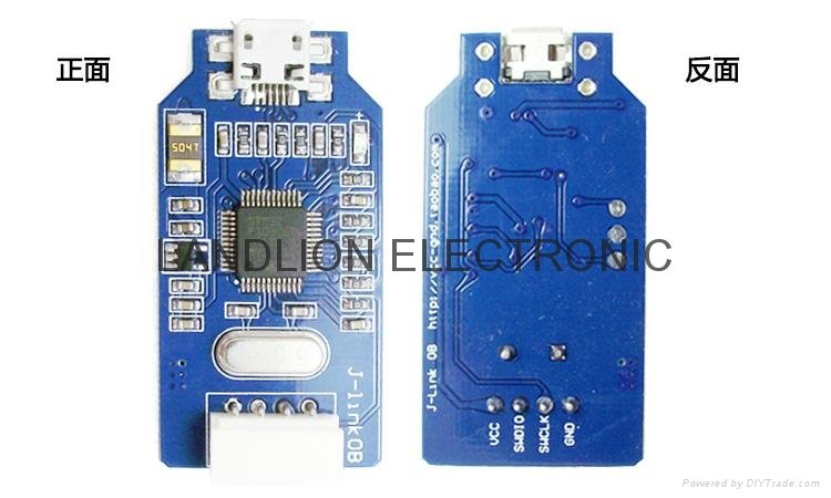
1, simplified interface, using four-wire: VCC, SWDIO, SWCLK, GND four interfaces, compared with JTAG, can save a number of IO port, complete high-speed debugging, download.
2, fully compatible with the traditional J-Link, with J-Link all the features.
3, the use of Mirco USB interface (currently the kind of smart phones), the data line common.
4,3.3V output, but also to the target board power supply, user-friendly debugging and download procedures.
5, onboard self-recovery fuse, to avoid short-circuit damage, so that the board more secure.
6, with a unique ID logo, multi-device debugging at the same time does not conflict.
7, the installation of transparent heat shrink tube, beautiful more intimate protection.
8, work is stable, no firmware loss phenomenon.
9, only U disk size, the circuit is simple, stable, reliable, easy to move and carry.
Payment Terms︰ TT Western union paypal
Product Image
